[Technology] Rethinking Thermal Management for High-Speed Optical Transceivers
As AI infrastructure scales, the transition to 1.6T and 3.2T optical transceivers introduces a strict engineering constraint: managing extreme heat flux within standardized hardware dimensions. Addireen addresses this thermal bottleneck through the monolithic integration of pure copper housings via advanced green-laser additive manufacturing.
The Heat Flux Dilemma in Standard Form Factors
The physical footprints of optical transceivers—dictated by standards like QSFP-DD and OSFP—remain unchanged, yet power consumption is escalating rapidly. While legacy 400G modules operate at roughly 10W, 1.6T architectures are projected to exceed 20W, and upcoming 3.2T designs may draw between 40W and 50W.
Furthermore, the industry's shift toward Linear-drive Pluggable Optics (LPO) and Co-Packaged Optics (CPO) places optical engines in closer proximity to switch ASICs, creating highly concentrated thermal zones. Localized overheating risks signal degradation, wavelength drift, and reduced component lifespans. Conventional forced-air cooling and traditional packaging materials are reaching their physical limits in mitigating these concentrated thermal loads.
Material Transition: The Efficiency of Pure Copper
With limited room for volumetric expansion, bulk material thermal conductivity dictates cooling efficiency. Pure copper delivers a thermal conductivity of 400 W/(m·K), significantly outperforming traditional alternatives like Kovar or tungsten-copper (W-Cu).
Replacing standard materials with a pure copper housing cuts junction-to-case thermal resistance by nearly half. This translates to a direct reduction in chip junction temperatures by 5°C to 10°C, providing a crucial thermal buffer for high-density optical components.
Structural Integration via Green-Laser AM
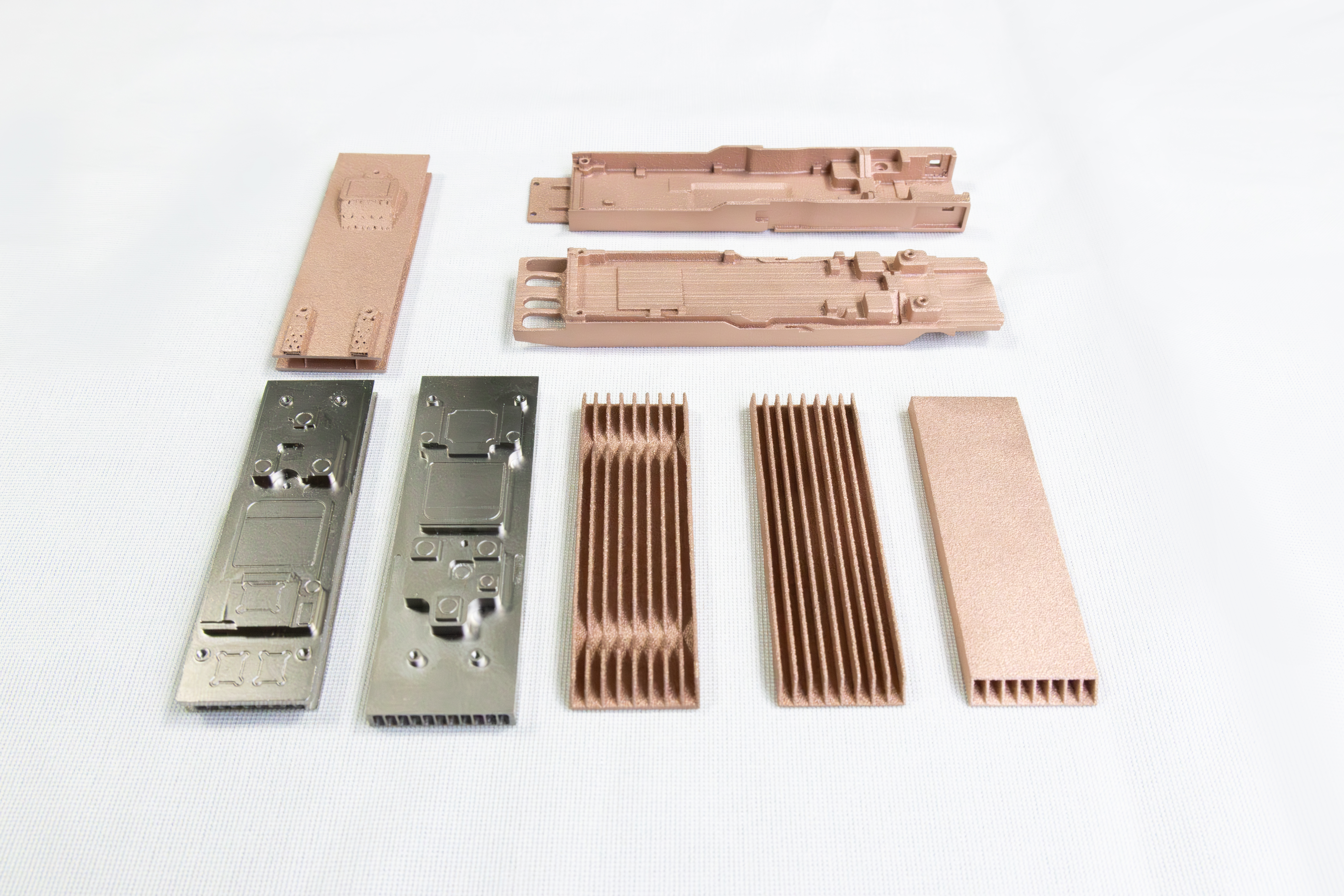
Processing highly reflective pure copper using standard near-infrared lasers results in poor energy absorption, leading to high porosity and manufacturing instability. Addireen bypasses this limitation by utilizing 532nm green-laser powder bed fusion. This specific wavelength ensures optimal energy absorption, stable melt pools, and high-density part consolidation with a minimum spot diameter of 15μm.
More importantly, this manufacturing process enables structural redesign rather than mere material substitution. It allows for the monolithic fabrication of intricate internal geometries—such as conformal cooling channels and ultra-thin, staggered short-fin arrays—directly inside the transceiver shell. The housing itself functions as an active heat sink, maximizing thermal dissipation without requiring modifications to the external assembly footprint.
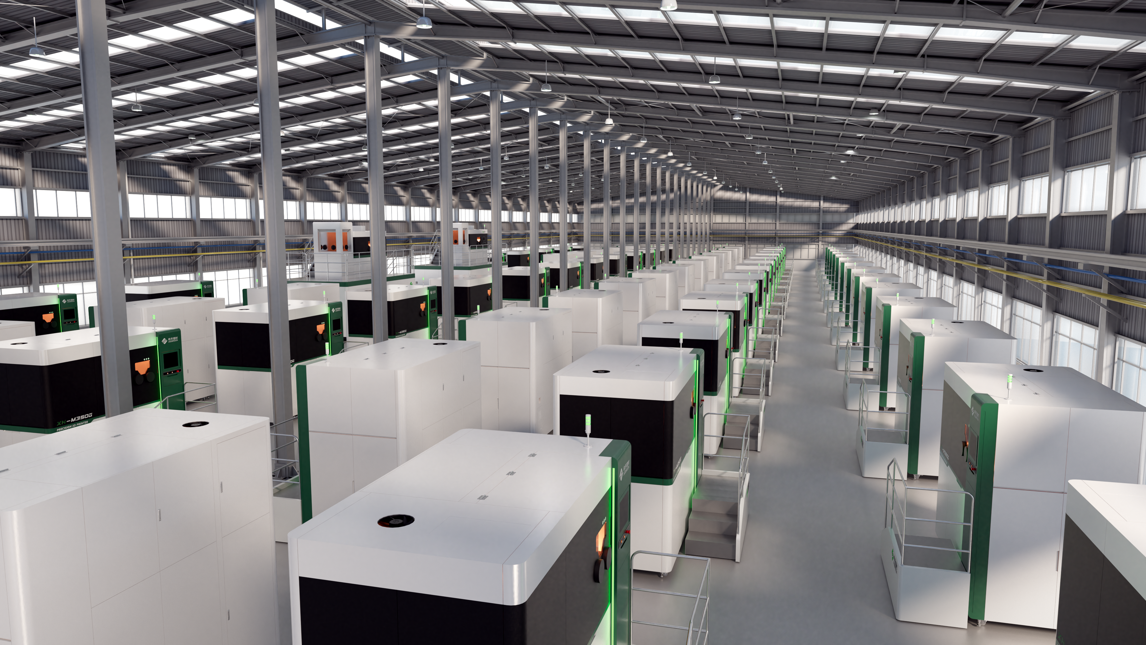
Ready for Volume Production
This solution is fully operational at an industrial scale. Addireen currently operates a production fleet of over 100 green-laser additive manufacturing systems, with strategic plans to expand to a 1,000-unit capacity.
By combining the thermal superiority of pure copper with the geometric freedom of 3D printing, Addireen provides a deployable thermal management framework for next-generation optical interconnects—requiring no custom tooling, no dimension alterations, and no disruption to existing assembly lines.